Diode


From Wikipedia, the free encyclopedia


The most common function of a diode is to allow an electric current to pass in one direction (called the diode's forward direction) while blocking current in the opposite direction (the reverse direction). Thus, the diode can be thought of as an electronic version of a check valve. This unidirectional behavior is called rectification, and is used to convert alternating current to direct current, and to extract modulation from radio signals in radio receivers.
However, diodes can have more complicated behavior than this simple on-off action, due to their complex non-linear electrical characteristics, which can be tailored by varying the construction of their P-N junction. These are exploited in special purpose diodes that perform many different functions. For example, specialized diodes are used to regulate voltage (Zener diodes), to electronically tune radio and TV receivers (varactor diodes), to generate radio frequency oscillations (tunnel diodes), and to produce light (light emitting diodes).
Diodes were the first semiconductor electronic devices. The discovery of crystals' rectifying abilities was made by German physicist Ferdinand Braun in 1874. The first semiconductor diodes, called cat's whisker diodes were made of crystals of minerals such as galena. Today most diodes are made of silicon, but other semiconductors such as germanium are sometimes used[2].
Contents[hide] |
[edit] History
Although the crystal semiconductor diode was popular before the thermionic diode, thermionic and solid state diodes were developed in parallel.The basic principle of operation of thermionic diodes was discovered by Frederick Guthrie in 1873.[3] Guthrie discovered that a positively charged electroscope could be discharged by bringing a grounded piece of white-hot metal close to it (but not actually touching it). The same did not apply to a negatively charged electroscope, indicating that the current flow was only possible in one direction.
Thomas Edison independently rediscovered the principle on February 13, 1880. At the time, Edison was carrying out research into why the filaments of his carbon-filament light bulbs nearly always burned out at the positive-connected end. He had a special bulb made with a metal plate sealed into the glass envelope, and he was able to confirm that an invisible current could be drawn from the glowing filament through the vacuum to the metal plate, but only when the plate was connected to the positive supply.
Edison devised a circuit where his modified light bulb more or less replaced the resistor in a DC voltmeter and, on this basis, was awarded a patent for it in 1883.[4] There was no apparent practical use for such a device at the time. So, the patent application was most likely simply a precaution in case someone else did find a use for the so-called “Edison Effect”.
About 20 years later, John Ambrose Fleming (scientific adviser to the Marconi Company and former Edison employee) realized that the Edison effect could be used as a precision radio detector. Fleming patented the first true thermionic diode in Britain [5] on November 16, 1904 (followed by U.S. Patent 803,684 in November 1905).
The principle of operation of crystal diodes was discovered in 1874 by the German scientist Karl Ferdinand Braun.[6] Braun patented the crystal rectifier in 1899.[7] Braun’s discovery was further developed by Jagdish Chandra Bose into a useful device for radio detection.
The first actual radio receiver using a crystal diode was built by Greenleaf Whittier Pickard. Pickard received a patent for a silicon crystal detector on November 20, 1906.[8]
Other experimenters tried a variety of minerals and other substances, although by far the most popular was the lead sulfide mineral Galena. Although other substances offered slightly better performance, galena had the advantage of being cheap and easy to obtain, and was used almost exclusively in home-built “crystal sets”, until the advent of inexpensive fixed-germanium diodes in the 1950s.
At the time of their invention, such devices were known as rectifiers. In 1919, William Henry Eccles coined the term diode from the Greek roots dia, meaning “through”, and ode (from ὅδος), meaning “path”.
[edit] Thermionic and gaseous state diodes

In thermionic valve diodes, a current through the heater filament indirectly heats the cathode, another internal electrode treated with a mixture of barium and strontium oxides, which are oxides of alkaline earth metals; these substances are chosen because they have a small work function. (Some valves use direct heating, in which a tungsten filament acts as both heater and cathode.) The heat causes thermionic emission of electrons into the vacuum. In forward operation, a surrounding metal electrode called the anode is positively charged so that it electrostatically attracts the emitted electrons. However, electrons are not easily released from the unheated anode surface when the voltage polarity is reversed. Hence, any reverse flow is negligible.
For much of the 20th century, thermionic valve diodes were used in analog signal applications, and as rectifiers in many power supplies. Today, valve diodes are only used in niche applications such as rectifiers in electric guitar and high-end audio amplifiers as well as specialized high-voltage equipment.
[edit] Semiconductor diodes
A modern semiconductor diode is made of a crystal of semiconductor like silicon that has impurities added to it to create a region on one side that contains negative charge carriers (electrons), called n-type semiconductor, and a region on the other side that contains positive charge carriers (holes), called p-type semiconductor. The diode's terminals are attached to each of these regions. The boundary within the crystal between these two regions, called a PN junction, is where the action of the diode takes place. The crystal conducts conventional current in a direction from the p-type side (called the anode) to the n-type side (called the cathode), but not in the opposite direction.Another type of semiconductor diode, the Schottky diode, is formed from the contact between a metal and a semiconductor rather than by a p-n junction.
[edit] Current–voltage characteristic
A semiconductor diode’s behavior in a circuit is given by its current–voltage characteristic, or I–V graph (see graph below). The shape of the curve is determined by the transport of charge carriers through the so-called depletion layer or depletion region that exists at the p-n junction between differing semiconductors. When a p-n junction is first created, conduction band (mobile) electrons from the N-doped region diffuse into the P-doped region where there is a large population of holes (vacant places for electrons) with which the electrons “recombine”. When a mobile electron recombines with a hole, both hole and electron vanish, leaving behind an immobile positively charged donor (dopant) on the N-side and negatively charged acceptor (dopant) on the P-side. The region around the p-n junction becomes depleted of charge carriers and thus behaves as an insulator.However, the width of the depletion region (called the depletion width) cannot grow without limit. For each electron-hole pair that recombines, a positively charged dopant ion is left behind in the N-doped region, and a negatively charged dopant ion is left behind in the P-doped region. As recombination proceeds more ions are created, an increasing electric field develops through the depletion zone which acts to slow and then finally stop recombination. At this point, there is a “built-in” potential across the depletion zone.
If an external voltage is placed across the diode with the same polarity as the built-in potential, the depletion zone continues to act as an insulator, preventing any significant electric current flow (unless electron/hole pairs are actively being created in the junction by, for instance, light. see photodiode). This is the reverse bias phenomenon. However, if the polarity of the external voltage opposes the built-in potential, recombination can once again proceed, resulting in substantial electric current through the p-n junction (i.e. substantial numbers of electrons and holes recombine at the junction). For silicon diodes, the built-in potential is approximately 0.7 V (0.3 V for Germanium and 0.2 V for Schottky). Thus, if an external current is passed through the diode, about 0.7 V will be developed across the diode such that the P-doped region is positive with respect to the N-doped region and the diode is said to be “turned on” as it has a forward bias.

Figure 5: I–V characteristics of a P-N junction diode (not to scale).
At very large reverse bias, beyond the peak inverse voltage or PIV, a process called reverse breakdown occurs which causes a large increase in current (i.e. a large number of electrons and holes are created at, and move away from the pn junction) that usually damages the device permanently. The avalanche diode is deliberately designed for use in the avalanche region. In the zener diode, the concept of PIV is not applicable. A zener diode contains a heavily doped p-n junction allowing electrons to tunnel from the valence band of the p-type material to the conduction band of the n-type material, such that the reverse voltage is “clamped” to a known value (called the zener voltage), and avalanche does not occur. Both devices, however, do have a limit to the maximum current and power in the clamped reverse voltage region. Also, following the end of forward conduction in any diode, there is reverse current for a short time. The device does not attain its full blocking capability until the reverse current ceases.
The second region, at reverse biases more positive than the PIV, has only a very small reverse saturation current. In the reverse bias region for a normal P-N rectifier diode, the current through the device is very low (in the µA range). However, this is temperature dependent, and at suffiently high temperatures, a substantial amount of reverse current can be observed (mA or more).
The third region is forward but small bias, where only a small forward current is conducted.
As the potential difference is increased above an arbitrarily defined “cut-in voltage” or “on-voltage” or “diode forward voltage drop (Vd)”, the diode current becomes appreciable (the level of current considered “appreciable” and the value of cut-in voltage depends on the application), and the diode presents a very low resistance. The current–voltage curve is exponential. In a normal silicon diode at rated currents, the arbitrary “cut-in” voltage is defined as 0.6 to 0.7 volts. The value is different for other diode types — Schottky diodes can be rated as low as 0.2 V, Germanium diodes 0.25-0.3 V, and red or blue light-emitting diodes (LEDs) can have values of 1.4 V and 4.0 V respectively.
At higher currents the forward voltage drop of the diode increases. A drop of 1 V to 1.5 V is typical at full rated current for power diodes.
[edit] Shockley diode equation
The Shockley ideal diode equation or the diode law (named after transistor co-inventor William Bradford Shockley, not to be confused with tetrode inventor Walter H. Schottky) gives the I–V characteristic of an ideal diode in either forward or reverse bias (or no bias). The equation is: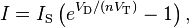
- I is the diode current,
- IS is the reverse bias saturation current (or scale current),
- VD is the voltage across the diode,
- VT is the thermal voltage, and
- n is the ideality factor, also known as the quality factor or sometimes emission coefficient. The ideality factor n varies from 1 to 2 depending on the fabrication process and semiconductor material and in many cases is assumed to be approximately equal to 1 (thus the notation n is omitted).

The Shockley ideal diode equation or the diode law is derived with the assumption that the only processes giving rise to the current in the diode are drift (due to electrical field), diffusion, and thermal recombination-generation. It also assumes that the recombination-generation (R-G) current in the depletion region is insignificant. This means that the Shockley equation doesn’t account for the processes involved in reverse breakdown and photon-assisted R-G. Additionally, it doesn’t describe the “leveling off” of the I–V curve at high forward bias due to internal resistance.
Under reverse bias voltages (see Figure 5) the exponential in the diode equation is negligible, and the current is a constant (negative) reverse current value of −IS. The reverse breakdown region is not modeled by the Shockley diode equation.
For even rather small forward bias voltages (see Figure 5) the exponential is very large because the thermal voltage is very small, so the subtracted ‘1’ in the diode equation is negligible and the forward diode current is often approximated as

[edit] Small-signal behaviour
For circuit design, a small-signal model of the diode behavior often proves useful. A specific example of diode modeling is discussed in the article on small-signal circuits.[edit] Types of semiconductor diode
| Diode | Zener diode | Schottky diode | Tunnel diode |
 | |||
| Light-emitting diode | Photodiode | Varicap | Silicon controlled rectifier |
Figure 6: Some diode symbols.


Normal (p-n) diodes, which operate as described above, are usually made of doped silicon or, more rarely, germanium. Before the development of modern silicon power rectifier diodes, cuprous oxide and later selenium was used; its low efficiency gave it a much higher forward voltage drop (typically 1.4–1.7 V per “cell”, with multiple cells stacked to increase the peak inverse voltage rating in high voltage rectifiers), and required a large heat sink (often an extension of the diode’s metal substrate), much larger than a silicon diode of the same current ratings would require. The vast majority of all diodes are the p-n diodes found in CMOS integrated circuits, which include two diodes per pin and many other internal diodes.
Avalanche diodes
- Diodes that conduct in the reverse direction when the reverse bias voltage exceeds the breakdown voltage. These are electrically very similar to Zener diodes, and are often mistakenly called Zener diodes, but break down by a different mechanism, the avalanche effect. This occurs when the reverse electric field across the p-n junction causes a wave of ionization, reminiscent of an avalanche, leading to a large current. Avalanche diodes are designed to break down at a well-defined reverse voltage without being destroyed. The difference between the avalanche diode (which has a reverse breakdown above about 6.2 V) and the Zener is that the channel length of the former exceeds the “mean free path” of the electrons, so there are collisions between them on the way out. The only practical difference is that the two types have temperature coefficients of opposite polarities.
- These are a type of point-contact diode. The cat’s whisker diode consists of a thin or sharpened metal wire pressed against a semiconducting crystal, typically galena or a piece of coal.[9] The wire forms the anode and the crystal forms the cathode. Cat’s whisker diodes were also called crystal diodes and found application in crystal radio receivers. Cat’s whisker diodes are generally obsolete, but may be available from a few manufacturers.[citation needed]
- These are actually a JFET[10] with the gate shorted to the source, and function like a two-terminal current-limiter analog to the Zener diode, which is limiting voltage. They allow a current through them to rise to a certain value, and then level off at a specific value. Also called CLDs, constant-current diodes, diode-connected transistors, or current-regulating diodes.
- These have a region of operation showing negative resistance caused by quantum tunneling, thus allowing amplification of signals and very simple bistable circuits. These diodes are also the type most resistant to nuclear radiation.
- These are similar to tunnel diodes in that they are made of materials such as GaAs or InP that exhibit a region of negative differential resistance. With appropriate biasing, dipole domains form and travel across the diode, allowing high frequency microwave oscillators to be built.
- In a diode formed from a direct band-gap semiconductor, such as gallium arsenide, carriers that cross the junction emit photons when they recombine with the majority carrier on the other side. Depending on the material, wavelengths (or colors)[11] from the infrared to the near ultraviolet may be produced[12]. The forward potential of these diodes depends on the wavelength of the emitted photons: 1.2 V corresponds to red, 2.4 V to violet. The first LEDs were red and yellow, and higher-frequency diodes have been developed over time. All LEDs produce incoherent, narrow-spectrum light; “white” LEDs are actually combinations of three LEDs of a different color, or a blue LED with a yellow scintillator coating. LEDs can also be used as low-efficiency photodiodes in signal applications. An LED may be paired with a photodiode or phototransistor in the same package, to form an opto-isolator.
- When an LED-like structure is contained in a resonant cavity formed by polishing the parallel end faces, a laser can be formed. Laser diodes are commonly used in optical storage devices and for high speed optical communication.
- These diodes are used as sensors, heat engines for thermoelectric cooling. Charge carriers absorb and emit their band gap energies as heat.
- All semiconductors are subject to optical charge carrier generation. This is typically an undesired effect, so most semiconductors are packaged in light blocking material. Photodiodes are intended to sense light(photodetector), so they are packaged in materials that allow light to pass, and are usually PIN (the kind of diode most sensitive to light)[13]. A photodiode can be used in solar cells, in photometry, or in optical communications. Multiple photodiodes may be packaged in a single device, either as a linear array or as a two-dimensional array. These arrays should not be confused with charge-coupled devices.
- These work the same as the junction semiconductor diodes described above, but their construction is simpler. A block of n-type semiconductor is built, and a conducting sharp-point contact made with some group-3 metal is placed in contact with the semiconductor. Some metal migrates into the semiconductor to make a small region of p-type semiconductor near the contact. The long-popular 1N34 germanium version is still used in radio receivers as a detector and occasionally in specialized analog electronics.
- A PIN diode has a central un-doped, or intrinsic, layer, forming a p-type/intrinsic/n-type structure[14]. They are used as radio frequency switches and attenuators. They are also used as large volume ionizing radiation detectors and as photodetectors. PIN diodes are also used in power electronics, as their central layer can withstand high voltages. Furthermore, the PIN structure can be found in many power semiconductor devices, such as IGBTs, power MOSFETs, and thyristors.
- Schottky diodes are constructed from a metal to semiconductor contact. They have a lower forward voltage drop than p-n junction diodes. Their forward voltage drop at forward currents of about 1 mA is in the range 0.15 V to 0.45 V, which makes them useful in voltage clamping applications and prevention of transistor saturation. They can also be used as low loss rectifiers although their reverse leakage current is generally higher than that of other diodes. Schottky diodes are majority carrier devices and so do not suffer from minority carrier storage problems that slow down many other diodes — so they have a faster “reverse recovery” than p-n junction diodes. They also tend to have much lower junction capacitance than p-n diodes which provides for high switching speeds and their use in high-speed circuitry and RF devices such as switched-mode power supply, mixers and detectors.
- Super barrier diodes are rectifier diodes that incorporate the low forward voltage drop of the Schottky diode with the surge-handling capability and low reverse leakage current of a normal p-n junction diode.
- As a dopant, gold (or platinum) acts as recombination centers, which help a fast recombination of minority carriers. This allows the diode to operate at signal frequencies, at the expense of a higher forward voltage drop. Gold doped diodes are faster than other p-n diodes (but not as fast as Schottky diodes). They also have less reverse-current leakage than Schottky diodes (but not as good as other p-n diodes).[15][16] A typical example is the 1N914.
- The term step recovery relates to the form of the reverse recovery characteristic of these devices. After a forward current has been passing in an SRD and the current is interrupted or reversed, the reverse conduction will cease very abruptly (as in a step waveform). SRDs can therefore provide very fast voltage transitions by the very sudden disappearance of the charge carriers.
- These are avalanche diodes designed specifically to protect other semiconductor devices from high-voltage transients[17]. Their p-n junctions have a much larger cross-sectional area than those of a normal diode, allowing them to conduct large currents to ground without sustaining damage.
- These are used as voltage-controlled capacitors. These are important in PLL (phase-locked loop) and FLL (frequency-locked loop) circuits, allowing tuning circuits, such as those in television receivers, to lock quickly, replacing older designs that took a long time to warm up and lock. A PLL is faster than an FLL, but prone to integer harmonic locking (if one attempts to lock to a broadband signal). They also enabled tunable oscillators in early discrete tuning of radios, where a cheap and stable, but fixed-frequency, crystal oscillator provided the reference frequency for a voltage-controlled oscillator.
- Diodes that can be made to conduct backwards. This effect, called Zener breakdown, occurs at a precisely defined voltage, allowing the diode to be used as a precision voltage reference. In practical voltage reference circuits Zener and switching diodes are connected in series and opposite directions to balance the temperature coefficient to near zero. Some devices labeled as high-voltage Zener diodes are actually avalanche diodes (see above). Two (equivalent) Zeners in series and in reverse order, in the same package, constitute a transient absorber (or Transorb, a registered trademark). The Zener diode is named for Dr. Clarence Melvin Zener of Southern Illinois University, inventor of the device.
[edit] Numbering and Coding schemes
There are a number of common, standard and manufacturer-driven numbering and coding schemes for diodes; the two most common being the EIA/JEDEC standard and the European Pro Electron standard:[edit] EIA/JEDEC
A standardized 1N-series numbering system was introduced in the US by EIA/JEDEC (Joint Electron Device Engineering Council) about 1960. Among the most popular in this series were: 1N34A/1N270 (Germanium signal), 1N914/1N4148 (Silicon signal), 1N4001-1N4007 (Silicon 1A power rectifier) and 1N54xx (Silicon 3A power rectifier)[18][19][20][edit] Pro Electron
The European Pro Electron coding system for active components was introduced in 1966 and comprises two letters followed by the part code. The first letter represents the semiconductor material used for the component (A = Germanium and B = Silicon) and the second letter represents the general function of the part (for diodes: A = low-power/signal, B = Variable capacitance, X = Multiplier, Y = Rectifier and Z = Voltage reference), for example:- AA-series germanium low-power/signal diodes (e.g.: AA119)
- BA-series silicon low-power/signal diodes (e.g.: BAT18 Silicon RF Switching Diode)
- BY-series silicon rectifier diodes (e.g.: BY127 1250V, 1A rectifier diode)
- BZ-series silicon zener diodes (e.g.: BZY88C4V7 4.7V zener diode)
- GD-series germanium diodes (ed: GD9) — this is a very old coding system
- OA-series germanium diodes (e.g.: OA47) — a coding sequence developed by Mullard, a UK company
- HP diode 1901-0044 = JEDEC 1N4148
- UK military diode CV448 = Mullard type OA81 = GEC type GEX23
No comments:
Post a Comment